
Document Type : Research Paper
INTRODUCTION
Surface plasmons, which are collective oscillations of free electrons at metal-dielectric interfaces, offer unique opportunities for confining light beyond the diffraction limit and enhancing light-matter interactions at the nanoscale [1-3]. This strong field confinement and enhancement make plasmonic waveguides promising for observing and exploiting third-order nonlinear optical effects, such as the Kerr effect [4-8]. Silicon-on-insulator (SOI) waveguides, compatible with complementary metal-oxide-semiconductor (CMOS) fabrication processes, have emerged as a promising platform for integrated photonic circuits. However, the intrinsically weak third-order nonlinearities of silicon limit the efficiency of nonlinear processes in conventional SOI waveguides [9, 10]. Integrating plasmonic structures with SOI waveguides can significantly enhance nonlinear effects by leveraging the strong field confinement and enhancement provided by surface plasmons [9-16].
The Kerr effect, which is a third-order nonlinear phenomenon, manifests as an intensity-dependent refractive index change in materials. This effect is particularly attractive for all-optical switching and signal processing applications, as it allows one optical signal to control the propagation of another through the modulation of the refractive index. Harnessing the Kerr effect in integrated photonic devices requires engineering structures that maximize the nonlinear interaction while minimizing detrimental effects, such as nonlinear absorption [17, 18]. Exploiting third-order nonlinear effects in plasmonic waveguides can lead to novel functionalities and improved performance in various applications, including all-optical switching [19, 20], signal regeneration [21], wavelength conversion [22], and optical signal processing [23]. However, achieving efficient nonlinear processes in plasmonic waveguides requires careful design considerations, such as optimizing mode confinement, minimizing propagation losses, and incorporating materials with large third-order nonlinear susceptibilities [24].
In recent years, the development of the study of plasmons in the two-dimensional material of graphene has received attention. The unique properties of graphene have led to its exploitation in photonic and optoelectronic devices [25]. Graphene-based nanomaterials have emerged as versatile platforms for a wide range of photonic and optoelectronic applications due to their unique electronic and optical properties, including high carrier mobility, tunable Fermi level, and strong light–matter interaction. These features enable their use in all-optical switches [26], modulators [27], logic gates [28],nanoscale sensors [29] and optical communication. The design of graphene-integrated hybrid plasmonic waveguides plays a critical role in maximizing nonlinear optical responses and device miniaturization. Various configurations, such as surface-deposited graphene, graphene-dielectric-graphene stacks, and multilayer hybrid architectures, have been explored to enhance Kerr nonlinearity and optical confinement.
Graphene contributes to the Kerr effect primarily due to its unique electronic structure and optical properties. The material’s conical band structure leads to a linear dispersion of electrons near the Dirac points, resulting in massless Dirac fermions that respond strongly to applied electric fields. Graphene’s high electron mobility allows for rapid response to optical fields, enhancing nonlinear optical effects. Both intraband and interband electronic transitions in graphene contribute to its nonlinear optical response, including the Kerr effect. The two-dimensional nature of graphene confines electrons to a plane, intensifying light-matter interactions and nonlinear optical effects. Additionally, the Fermi level of graphene can be easily tuned by electrical gating or chemical doping, allowing for control over its nonlinear optical properties, including the Kerr effect. These factors collectively enhance graphene’s contribution to the Kerr effect, making it a promising material for nonlinear optical applications [30-37].
Kerr nonlinear response of graphene is reported in many works [38-42]. In this research , the dielectric - graphene - dielectric structures have been analyzed using theoretical and experimental approaches. Additionally, the behavior of these structures is simulated using finite element method (FEM) using COMSOL Multiphysics software [30]. Kim et al. [42] demonstrated plasmonic waveguides using graphene in 2011. Thakur et al., and Kang et al. [39, 40] investigated Kerr nonlinear response of graphene in 2019 and 2020, respectively. In [31], a thin graphene nanoribbon sandwiched between two silicon dioxide layers enabled the formation of a plasmonic waveguide near the graphene, exhibiting good optical confinement and a low channel loss of 0.029 dB/μm. Additionally, graphene’s linear band structure, which is characterized by the Dirac-like conical energy dispersion near the Dirac points, is theorized to give rise to large nonlinear optical effects, spurring significant research efforts in graphene nonlinear optics [32-37]. A novel dielectric-loaded graphene three-waveguide coupler based on stimulated Raman adiabatic passage (STIRAP) has also been proposed [43], demonstrating resilience to geometric disturbances and potential for use in compact optical devices for computing and biosensing. In [44], the authors proposed nonlinear graphene-loaded deep-subwavelength plasmonic waveguides with a footprint of 30 × 20 nm2 for an energy-efficient all-optical switch with a switching energy of 35 fJ and a switching time of 260 fs. Ojaghi et al. [45] designed graphene-based all-optical modulators, exploiting graphene’s Kerr nonlinearity to achieve compact devices with high modulation depths. In [46], the authors theoretically investigated and optimized the Kerr nonlinear optical performance of silicon-on-insulator (SOI) nanowires integrated with 2D layered graphene oxide (GO) films. They demonstrated that the effective nonlinear parameter could be significantly enhanced by incorporating the GO films. Rahimi et al. [38] proposed a novel plasmonic structure, which includes graphene, for developing a wedge hybrid plasmonic waveguide for Kerr nonlinear applications. They achieved the maximum nonlinear coefficient of 2.68 × 10⁷ W−1km−1, and Kerr nonlinear FoM of 0.029. Zhang et al. [41] designed a graphene oxide-silicon (GO-Si) waveguides that obtained a nonlinear coefficient of 668 W−1m−1 for a waveguide area of just 0.11 μm2.
Despite the significant progress in graphene-assisted and hybrid plasmonic waveguides, a critical challenge remains unresolved: how to simultaneously achieve strong Kerr nonlinear enhancement, low propagation loss, and ultra-compact device dimensions within a fabrication-feasible structure. In many previously reported designs, graphene is either used as a surface conductivity enhancer or integrated in configurations that do not fully maximize its overlap with highly nonlinear dielectric media. Consequently, the nonlinear interaction strength is not optimally exploited, and the confinement–loss trade-off persists. To address this limitation, we propose a structurally optimized nonlinear graphene hybrid plasmonic waveguide (NGHPW) in which a graphene monolayer is strategically embedded between two nonlinear DDMEBT layers beneath a thin silver cap on a silicon-on-insulator (SOI) platform. This configuration enhances the spatial overlap between the plasmonic field, graphene-induced nonlinear response, and the nonlinear dielectric medium, thereby significantly strengthening the Kerr interaction while maintaining structural simplicity. The high nonlinear coefficient arises from the combined effects of strong plasmonic field enhancement and the large third-order nonlinear susceptibilities of both the nonlinear media and graphene.
We utilize a figure-of-merit (FoM) parameter to evaluate the overall NGHPW performance as a function of the nonlinear coefficient (γ), propagation length (LP), input threshold power (P0,th), and confinement factor (Γ). Numerical results obtained using the finite element method (FEM) show that, regardless of propagation length and mode area, the nonlinear coefficient (γ) and FOM improve for smaller gap thicknesses. As an application, we designed and simulated a directional coupler consisting of two parallel NGHPWs, demonstrating its suitability for compact optical devices. As for the improvements of this work compared to the previous one in Ref. [47], we can highlight the reduced complexity in fabrication, which makes the new structure more practical for real-world applications. Additionally, the competitive level of nonlinearity maintained in the proposed structure, despite the reduction in complexity, making it a more feasible solution for practical implementation. Therefore, the proposed approach reduces fabrication complexity while maintaining competitive nonlinearity, offering a feasible solution for integrated optical applications.
SCHEMATIC AND SPECIFICATIONS OF NGHPW
A crucial preliminary step in designing optical components with efficient Kerr performance is the systematic design of the nonlinear waveguide through which light propagates. This process involves several key considerations and steps. First, we identify the design drivers: two key elements driving the design of such waveguides are minimizing the effect of two-photon absorption (TPA) in silicon [48] and maximizing the overlap between the propagating optical mode and the nonlinear materials deposited on the silicon waveguide. These constraints then guide our choice towards waveguiding structures with high field confinement within the nonlinear materials. To satisfy these design requirements, we select appropriate materials, employing a multi-layer structure for the gap region consisting of two layers of DDMEBT with a single graphene layer sandwiched in between. The waveguide geometry is then optimized, with its cross-section carefully designed to balance the competing requirements of minimizing TPA and maximizing nonlinear interaction. Electromagnetic simulations are performed to verify the field confinement and optimize the layer thicknesses for maximum nonlinear effect. Finally, based on the simulation results and practical fabrication constraints, we determine the final waveguide structure. The cross-section of the considered waveguide geometry, resulting from this step-by-step design process, is shown in Fig. 1.
The thicknesses of the thin DDMEBT layers and the single graphene layer in between are labeled as hnl and tg, respectively. The thickness of the metal cap is denoted as hAg, and the waveguide width is set to W = 100 nm. To identify the propagation conditions and evaluate the modal overlap factor with the nonlinear materials, we calculated the mode profiles at a wavelength of 1550 nm using a finite element mode solver (COMSOL Multiphysics). The simulated parameters of the related waveguide materials and geometries are listed in Table 1.
The complex surface conductivity of graphene is calculated as the sum of contributions from intraband and interband transitions, expressed as 𝜎 (𝜔)= 𝜎intra + 𝜎inter, where 𝜎intra accounts for intraband electron-phonon scattering processes, and 𝜎inter represents interband transitions. The frequency-dependent optical conductivity of graphene, σ(ω), considering both intraband and interband optical transitions, can be derived from the Kubo formalism [54, 55] and is given by Eq. 1.

Here, e is the electron charge, ħ is the reduced Planck constant, 𝜇 is the Fermi-Dirac level, τ is the relaxation time accounting for various scattering mechanisms, 𝜔 is the angular frequency, kB is the Boltzmann constant, and T is temperature. The intraband contribution, σintra, arises from the transitions within the same conduction or valence band and is proportional to the Drude-like term, while the interband contribution, σinter, originates from the vertical transitions between the valence and conduction bands, leading to absorption and nonlinear effects. By using Eq. 1, the refractive index of graphene ng=√(1+(iσ(ω)/(ωε0tg) is calculated as a single layer with a thickness of tg=0.35 nm and ε0 is the permittivity of free space. The nonlinear refractive index (n2) of graphene used in this study is 1×10-11 m2/W, a value widely accepted in the literature for monolayer graphene under typical conditions. It’s important to note that this value represents an average for undoped graphene. The nonlinear coefficient of graphene can vary with the Fermi level due to its unique band structure and its effect on the material’s optical response. This Fermi level dependence is a crucial consideration for precise device engineering, as it allows for potential tuning of the nonlinear optical properties.
METHOD OF ANALYSIS
In this section, we focus on the nonlinear Kerr effect and examine the parameters influencing its behavior. When materials with permanent or induced dipole moments are subjected to an optical field, the dipoles tend to reorient themselves along the direction of the applied field. However, this reorientation process is much slower than the oscillation of the optical field itself. Nonetheless, the optical field contains a static (ω = 0) component, known as optical rectification, which can induce molecular reorientation. After this electronic and nuclear reorientation occurs, the material no longer exhibits isotropic properties, and the refractive index along the direction of the optical electric field becomes different from the refractive indices in other directions. This anisotropy in the refractive index, known as birefringence, increases with the square of the electric field amplitude, |E|2, which is proportional to the light intensity, I. This intensity-dependent birefringence is referred to as the optical Kerr effect. The optical Kerr effect can be described by the Eq. 2:
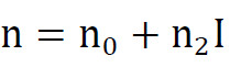
Where n is the refractive index, n0 is the linear refractive index, and n2 is the nonlinear refractive index coefficient, also known as the Kerr coefficient. The Kerr coefficient quantifies the magnitude of the intensity-dependent refractive index change induced by the optical Kerr effect. The values of n2 and n0 of the proposed waveguide materials are listed in Table 1.
The attenuation characteristics of a waveguide are governed by the wavelength dependence of the mode propagation length. The propagation length is defined as the distance along the z-axis over which the power amplitude of an electromagnetic mode decays by a factor of 1/e [56]. The propagation length, LP, can be obtained from the Eq. 3:
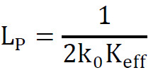
where k0 is the free-space wavenumber, and Keff is the imaginary part of the effective mode index.
The effective mode area, Aeff, is defined as the equivalent cross-sectional area through which the electromagnetic power propagates, and it is formulated using the Eq. 4 [57]:
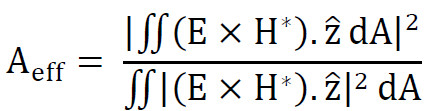
Where E and H are the electric and magnetic field vectors, respectively, and z ̂ is the unit vector along the propagation direction.
To quantify the Kerr nonlinearity in the waveguide, the nonlinear coefficient γ is often used to evaluate the magnitude of the nonlinearity. According to the full vector nonlinear model, γ for a sub-wavelength waveguide is defined as Eq. 5 [58]:
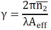
Here, λ is the optical wavelength in free space, and n̅2 is the nonlinear refractive index averaged over the inhomogeneous cross-section, weighted by the field distribution. The averaged nonlinear refractive index, n̅2, is expressed as Eq. 6 [59]:

To determine the electric field distributions of the propagating modes in the waveguide material, we estimated their confinement factors, Γ, in the waveguide layer according to Eq. 7:
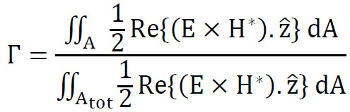
where A represents the desired region, and Atot represents the full waveguide cross-section.
To evaluate the effectiveness of inserting graphene on the Kerr nonlinear effect in the proposed waveguide, we have used the figure of merit reported in Ref. [60] as Eq. 8:
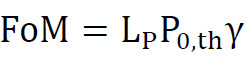
Where P0,th=AeffP Ith is the allowable damage threshold input optical power which AeffP is effective area for mode power. Also Ith is damage threshold intensity therefore input power should be chosen carefully so that the intensity in the sub-wavelength core domain remains lower than the damage threshold of the material. In our proposed waveguide, power limitation comes from DDMEBT polymer, beyond this value the polymer will get damaged. The intensity threshold was obtained for DDMEBT layer Ith= 5 GWcm-1 [60]. In equation 8, γ is the total nonlinear coefficient, which is calculated as Eq. 9:
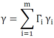
where m is the number of nonlinear layers of interest in the waveguide, γi is the nonlinear coefficient of the i-th layer, and Γi is the confinement factor of the mode in the i-th layer. In this paper, the nonlinear effect of the silver layer is ignored.
RESULTS AND DISCUSSION
Numerical simulations of the NGHPW were conducted using the finite element method (FEM) implemented within the COMSOL Multiphysics software package. The computational domain was discretized utilizing a triangular mesh with a minimum element size of 0.02 nm, ensuring geometric fidelity. The analysis employed a full-vectorial approach based on the electric field formulation.
Fig. 2 illustrates the real and imaginary components of graphene’s refractive index at telecommunication wavelengths. The real part of the refractive index reaches its maximum value around 0.4eV, then steadily decreases, while the imaginary part intersects it at approximately 0.47eV. For energy levels below 0.47eV, graphene behaves like a dielectric material. However, when the energy exceeds 0.47eV, graphene exhibits metallic properties due to the dominance of interband transitions over intraband transitions [54]. From Fig. 2, it is evident that graphene’s optical absorption increases for energies greater than 0.47eV, attributable to its metallic nature.
Fig. 3 depicts the electric field distribution (|E|) of the fundamental transverse magnetic (TM) mode at the operating wavelength of 1.55 μm in the proposed NGHPW. The waveguide structure incorporates a graphene layer sandwiched between two dielectric layers of DDMEBT. The high concentration of the electric field in the vicinity of the graphene layer effectively confines the optical mode, preventing leakage into the surrounding regions. This confinement leads to a significant enhancement of surface plasmon polaritons (SPPs) within the waveguide core. The strong mode confinement improves the guiding characteristics of the surface plasmon polaritons and consequently increases the efficiency of the nonlinear Kerr effect. It can be qualitatively observed that a substantial fraction of the propagating mode power is localized within the sub-wavelength DDMEBT gap regions. Consequently, the proposed structure facilitates an enhanced interaction between the graphene layer and the electric field, as the DDMEBT-graphene-DDMEBT layers are strategically positioned within the low-index gap regions, where the field intensity is maximized. Additionally, Fig. 3 presents a one-dimensional plot of the y-component of the electric field distribution along the x and y directions. It is evident that the mode is strongly confined in the y-direction near the graphene layer, resulting in an increased field enhancement within the two DDMEBT regions. This field enhancement is crucial for exploiting the nonlinear properties of the materials and achieving efficient nonlinear optical processes.
Fig. 4 presents the simulation results for the effective index, modal propagation length, normalized effective mode area, and threshold power of the fundamental mode in the NGHPW structure. These parameters are analyzed as a function of the DDMEBT thickness (hnl) and waveguide width (W = 100nm, 200nm, 300nm) when the chemical potential (μ) is 0.5eV. As depicted in Fig. 4a, increasing the DDMEBT thickness and decreasing the waveguide width results in a reduction of the real part of the effective mode index. Consequently, less optical power is concentrated within the nonlinear DDMEBT layers. Fig. 4b illustrates that decreasing the DDMEBT thickness and waveguide width leads to a smaller effective mode area. Since the field enhancement factor is inversely proportional to the mode volume, this reduced effective area significantly increases the electric field enhancement factor, thereby enhancing the observation of nonlinear effects. This characteristic suggests that the proposed NGHPW could serve as a plasmonic optical device, providing a small effective area suitable for compact components. However, for the wider waveguide (e.g., W = 300 nm), the effective area exhibits an almost linear variation with respect to the gap size. In contrast, for smaller waveguide widths, the effective area saturates as the DDMEBT layer thickness increases, as more light cannot be concentrated in the nonlinear region. The simulation results in Fig. 4c reveal that the modal attenuation sensitivity is more pronounced for wider waveguides (W = 200 and 300 nm) compared to W = 100 nm. This behavior is attributed to a larger portion of the optical field within the graphene layer and its interface with the silver layer for wider waveguides.
The confinement factor (Γ) quantifies the ratio of optical power confined within a specific region of the waveguide to the total optical power of each mode. Fig. 5a illustrates the confinement factor of the waveguide layer with respect to the DDMEBT layer thickness for the fundamental TM mode. For a DDMEBT thickness of hnl = 5 nm, the confinement factors in the top and bottom DDMEBT layers are calculated to be Γ = 0.063 and Γ = 0.057, respectively. The simulation results indicate that the optical power confined in the top DDMEBT layer is higher than in the bottom DDMEBT layer. This behavior can be attributed to the increased concentration of light at the interface between the silver (Ag) layer and the DDMEBT layer.
Fig. 5b depicts the averaged nonlinear indices (n̅2) of the waveguide layers as a function of the DDMEBT thickness (hnl). The simulation results indicate that the maximum nonlinear index is observed in the graphene layer, followed by the DDMEBT, silicon (Si), and silicon dioxide (SiO2) layers, respectively. This trend is attributed to the intrinsically higher nonlinearity of these materials. While the optical fields present in each layer can potentially influence the averaged nonlinear index (n̅2), the substantial difference in nonlinearity between the utilized materials minimizes this effect. In other words, the higher nonlinearity of certain layers, such as graphene and DDMEBT, dominates the overall nonlinear response, effectively mitigating the influence of the optical field distribution across the layers.
The nonlinear coefficient (γ) of the bare waveguides was estimated from the nonlinear refractive index and the effective mode area of the propagating mode within the waveguide, using Eq. 9. The minimum effective mode area (Aeff) was numerically evaluated from the field profile, yielding a value of approximately 0.032 μm2 based on the standard definition given by Eq. 4. This value is significantly smaller compared to the reference [58]. To provide a rough estimate of the nonlinear coefficient for the waveguides covered by graphene, graphene was treated as a thin layer with a thickness of tg = 0.35 nm sandwiched between two DDMEBT layers. For a waveguide with hnl = 5 nm and a width of W = 100 nm, the nonlinear coefficient was found to be γ = 3.99 × 10⁸ W-1km-1. Fig. 5c illustrates the nonlinear coefficient (γ) of the NGHPW as a function of the DDMEBT thickness (hnl). The simulation results indicate that the nonlinear coefficient decreases with increasing hnl due to reduced confinement and an expansion of the effective mode area. Fig. 5d investigates the impact of the gap height (hnl) and waveguide width (W) in the NGHPW on its Kerr nonlinear performance. The figure of merit (FoM) for different waveguide widths is plotted as a function of hnl to evaluate the Kerr nonlinear performance. The simulation results indicate that as the gap height increases, the electric field distribution at the graphene layer gradually distorts, with more optical power concentrating in the silicon and DDMEBT regions. Consequently, the effective mode area increases, significantly reducing the nonlinear interaction. Therefore, it can be summarized that the proposed NGHPW exhibits better Kerr nonlinear performance with a thinner gap size. However, excessively thin gaps may not be feasible due to fabrication constraints. On the other hand, reducing the waveguide width can also decrease the effective mode area, which will increase the FoM. The maximum FoM of 0.024, corresponding to the highest efficiency of the Kerr nonlinear effect, is obtained for hnl = 5 nm and W = 100 nm. As shown in Fig. 5d, in comparison to the conventional hybrid plasmonic waveguide (HPW) reported in reference [60] (represented by the dashed line), the proposed NGHPW configuration demonstrates superior performance for smaller dimensions (hnl < 15 nm). This characteristic makes the NGHPW suitable for compact optical circuits in all-optical devices.
To contextualize our simulation results, we compare the proposed NGHPW with other recent designs. Table 2 provides a comparative overview of the proposed NGHPW and selected previously published works, highlighting the novelty, enhanced nonlinear performance, and practical advantages of our design. In this table, summarizes the key characteristics of various waveguide structures, including nonlinear coefficient, propagation length, normalized effective area , and FoM. Based on the results, the proposed nonlinear graphene hybrid plasmonic waveguide (NGHPW) significantly enhances Kerr nonlinearity while maintaining a compact footprint, which is superior to conventional SOI or graphene-based waveguides. Unlike previous works, which often suffer from either limited nonlinearity, larger device size, or fabrication complexity, our design strategically integrates graphene between nonlinear DDMEBT layers, achieving a high nonlinear coefficient (γ = 3.99 × 10⁸ W-1km-1) and an ultra-small effective mode area (0.032 μm2). Moreover, the FoM incorporating γ, propagation length, and confinement factor, confirms improved overall nonlinear performance. In comparison to other works, our study provides a balanced combination of high nonlinearity, compactness, and fabrication feasibility, which represents a meaningful advancement in integrated nonlinear photonics.
Fabrication Feasibility
The fabrication of the proposed hybrid nonlinear waveguide structure, while challenging, is feasible using state-of-the-art nanofabrication techniques. The process would begin with a standard silicon-on-insulator (SOI) wafer as the base substrate. The silicon ridge waveguide can be patterned using electron-beam lithography followed by reactive ion etching. For the DDMEBT layers, molecular beam epitaxy (MBE) or organic vapor phase deposition (OVPD) can be employed to achieve precise thickness control. The graphene monolayer can be grown separately via chemical vapor deposition (CVD) on copper foil and then transferred onto the first DDMEBT layer using a wet transfer method with PMMA as a support layer. After transfer, the PMMA can be removed with acetone. The second DDMEBT layer can then be deposited using the same technique as the first. For the thin silver cap, electron-beam evaporation or sputtering can be used to achieve a uniform, thin layer. Each step of the fabrication process would require careful optimization to ensure the quality and integrity of each layer [61, 62].
COUPLNG MECHANISMS: DIRECTIONAL AND BUTT-COUPHING ANALYSIS
A directional coupler comprises two waveguides separated by a small gap, allowing evanescent coupling of light from one waveguide to the other over a characteristic coupling length. However, the direct application of directional coupling in plasmonics is limited by this characteristic length. Previous studies have demonstrated plasmonic directional couplers with coupling lengths as short as 410 µm for long-range surface plasmons at a wavelength of 1.55 μm, where the waveguides were separated by 4 μm. Numerous theoretical and experimental investigations have explored directional coupling between photonic and plasmonic waveguides of various geometries, employing high-index dielectrics or complex layered dielectric/metallic structures to compensate for the plasmonic dispersion [64-67].
Fig. 6a illustrates our proposed directional coupling configuration between a conventional SOI-based plasmonic waveguide and our nonlinear hybrid plasmonic waveguide. The simulations were performed at a telecommunications wavelength of 1.55 μm, with graphene’s chemical potential (μ) fixed at 0.5 eV. The nonlinear hybrid plasmonic waveguide comprises the following layers: a nonlinear material layer with thickness hnl = 5 nm, a silicon ridge of width W = 100 nm and height tSi = 220 nm, a silicon dioxide substrate of thickness hsub = 200 nm, and a graphene layer of thickness tg = 0.35 nm. The adjacent SOI-based plasmonic waveguide maintains the same ridge width (W) and similar layer configuration as the nonlinear structure, with the key difference being its SiO2 layer thickness (hd), which equals tg + 2hnl. The coupling strength between these waveguides is controlled by the spacing distance D between them. This configuration enables efficient power transfer from the conventional SOI-based plasmonic waveguide to our proposed nonlinear structure, facilitating practical integration with existing photonic circuits.
The simulation results for the supermodes obtained in the directional coupler structure are presented in Figs. 6b and 6c. The supermodes can be identified by examining the direction of the electric field vectors (represented by arrows). In Fig. 6b, the electric field vectors through both waveguides are aligned in the same direction, indicating the even supermode. Conversely, in Fig. 6c, the arrows point in opposite directions, signifying the odd supermode. The coupling length (Lc) can be related to the propagation constants of the even and odd modes in the nonlinear directional coupler through the Eq. 10 [68]:
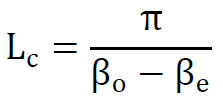
where βe and βo represent the propagation constants for the even and odd eigenmodes, respectively. Using the COMSOL optical mode solver, the propagation constants of the even and odd TM supermodes in the coupling region were calculated. Subsequently, the coupling length Lc was determined by substituting these values into Eq. (10).
The simulation results presented in Fig. 6d reveal that the coupling length (Lc) increases exponentially as the separation distance (D) between the two waveguides in the directional coupler increases. Consequently, a longer coupling length is required for larger separation distances between the waveguides. Notably, for a separation distance of D = 100 nm, the coupling length is as small as 2.5 μm. This characteristic of achieving extremely short coupling lengths highlights the promising potential of the proposed NGHPW system in the fields of nanophotonics and integrated optics.
The investigation of a directional coupler based on our proposed nonlinear hybrid waveguide is essential for its integration into SOI-based photonic circuits. This analysis provides crucial insights into the coupling dynamics of our unique structure, which combines plasmonic, dielectric, and 2D materials, and its potential performance in coupled-waveguide systems such as ring resonators and Mach-Zehnder interferometers. Understanding these coupling characteristics is fundamental for expanding the structure’s applications in integrated nonlinear optics.
To investigate the feasibility of direct integration with conventional silicon photonics platforms, we analyzed the butt-coupling [68, 69] between a standard SOI waveguide and our proposed nonlinear structure using Lumerical FDTD simulations (Fig. 7a). The simulation domain consisted of a 2 μm-long SOI waveguide directly connected to a 5 μm-long section of our nonlinear structure. The fundamental TM mode was excited at the input of the SOI waveguide (Fig. 7b), and the power distribution was monitored throughout the structure in both xy- and yz-planes Fig. 7c and 7d.
The simulation results reveal several key characteristics of the coupling mechanism. The xy-plane power distribution at the input confirms the excitation of the fundamental TM mode in the SOI waveguide. The yz-plane visualization of power propagation demonstrates the transition of optical power from the SOI waveguide to the nonlinear structure, where the mode exhibits a characteristic twin-waveguide behavior due to the hybridization of plasmonic and dielectric modes. Analysis of the power distribution along a cutline through the Si layer (Fig. 7d) reveals minimal back-reflection at the interface between the SOI waveguide and the nonlinear structure, indicating reasonable mode matching. However, as expected from the plasmonic nature of our structure and the presence of the graphene layer, the optical power shows exponential decay along the propagation direction in the nonlinear section, which is consistent with the inherent loss characteristics of plasmonic waveguides.
To summarize, the simulation results demonstrate that the proposed NGHPW structure significantly enhances the Kerr nonlinear effect, achieving a high nonlinear coefficient of γ = 3.99 × 10⁸ W⁻¹km⁻¹ and a minimum effective mode area of 0.032 μm². These findings directly address the identified research gap in achieving strong nonlinear interaction within compact plasmonic waveguides. By optimizing the waveguide geometry, including DDMEBT layer thickness and waveguide width, we improve field confinement and nonlinear response, providing a clear solution to the challenge of realizing high-performance, miniaturized nonlinear photonic devices. Additionally, the realization of a 2.5 μm coupling length in the designed directional coupler confirms that the enhanced Kerr effect is not merely a numerical improvement but translates into tangible device-level compactness. Furthermore, practical coupling configurations demonstrate that the proposed design is compatible with existing silicon photonic platforms, emphasizing its importance for integrated optics applications such as switches, modulators, and couplers. Overall, these findings validate the proposed structural strategy and demonstrate its value for next-generation integrated nonlinear nanophotonic devices.
CONCLUSION
In this work, we proposed and numerically investigated a nonlinear graphene hybrid plasmonic waveguide (NGHPW) with a graphene monolayer embedded between two DDMEBT layers on an SOI platform. Finite element simulations demonstrated a high nonlinear coefficient (γ = 3.99 × 10⁸ W⁻¹km⁻¹) and a subwavelength effective mode area (0.032 μm²), confirming enhanced Kerr nonlinearity and strong field confinement. Optimized waveguide geometry further improved nonlinear interaction without significantly compromising propagation length. Device-level validation through an ultra-compact directional coupler (2.5 μm coupling length) and butt-coupling to conventional SOI waveguides illustrates practical integration potential. These results demonstrate that strategic graphene placement effectively enhances Kerr nonlinearity while maintaining compactness, highlighting the NGHPW as a promising platform for integrated nonlinear photonic devices, including switches, modulators, and compact optical circuits.
CONFLICT OF INTEREST
The authors declare that there is no conflict of interests regarding the publication of this manuscript.
