
Document Type : Research Paper
INTRODUCTION
Nanomaterials are defined as materials that possess at least one dimension in the nanoscale range (1–100 nm). Due to the high surface-to-volume ratio and quantum size effects, they show different physical and chemical properties in relation to their ligand forms at this scale. These distinctive features have resulted in broad interest in nanomaterials for diverse applications, such as electronics, energy, catalysis, and especially gas sensing [1]. Nanotechnology is the science and technology that deals with designing, controlling, and applying materials at the nano level. It allows for the precise manipulation of matter at atomic and molecular scales to create structures with improved or entirely new properties. And this has offered sources of opportunities in diverse sectors, including healthcare, electronics, power generation, and eco-friendly applications. Nanotechnology is one of the most important tools for gas sensing devices; it improves material performance, provides high sensitivity, and allows us to develop low-cost and efficient sensors based on nanostructured materials [2]. Zinc oxide (ZnO) is one of the most important n-type semiconductor metal oxides, with features such as a wide band gap (~3.37 eV), high surface reactivity, and good chemical stability. Such characteristics make ZnO a good candidate for gas sensing purposes. Yet, it still needs to be improved in sensitivity, selectivity, and operating temperature when sensing [3]. To improve the sensing characteristics of ZnO, several modification strategies have been employed, and noble metal doping is one of its most efficient methods. The generation of silver (Ag) nanoparticles offers a promising platform for enhancing surface reactivity through better oxygen adsorption, ultimately improving the charge transfer processes and significantly impacting both sensor response and performance [4,5]. In this contribution, the gas sensing response of Ag-doped ZnO thin films prepared via spin coating at variable operating temperatures towards NO₂ was systematically studied from 25 °C to 200 °C, thus enabling the interrelation of both doping and temperature effects on sensor performance in detail [6]. This study differs from previous reports in several aspects. First, the fabrication of Ag–ZnO thin films was carried out using the spin coating method, which provides a simple and cost-effective approach for film deposition. Second, a comparative analysis of gas sensing performance at multiple operating temperatures was performed rather than focusing on a single temperature, as commonly reported in the literature. Finally, the combination of Ag doping with a comprehensive temperature-dependent study provides deeper insight into the sensing mechanism and significantly enhances the overall performance, making Ag–ZnO a promising material for efficient NO₂ gas detection. The goal is to explore the impacts of silver (Ag) doping and thermal annealing on structural, optical, and gas sensing properties of ZnO thin films. Moreover, its objective is to increase the surface area and adsorption sites to improve ZnO performance for NO₂ gas sensing.
MATERIALS AND METHODS
Chemicals
In this Work, Zinc Oxide (ZnO) and silver (Ag) were used as starting materials. Zno was obtained as a Nano powder with a particle size ranging from 10 to 30 nm from PanVace Sky Spring Nanomaterials, Inc., with a purity (99.8%). Silver Powder (Ag)was also used, as powder with an average particle size (APS) of 149 \mu m from Sigma-Aldrich (Merck KGaA, Germany) and high purity (99.9%).
Synthesis of Pure and Ag-Doped ZnO Thin Films
This method, Spin Coating, has been used for depositing thin films and for controlling the film morphology. The film’s properties and quality are determined by process parameters. Preparation of Thin Films at Partner Institution: Create thin films in a specially configured spin coating setup (model V T C-100) that is available at the partner institution, University of Babylon / Faculty of Basic Education. The system is configured with several components that were utilized to assist in the fabrication of a range of films on various substrates. By manipulating the speed and timing of the rotation of the frame. It is possible to adjust the thickness of the films synthesized in this system. Oil film thickness for the system decreases with an increase in the rotational speed and vice versa. Rotational speed, stability, and balance of the system also affect the uniformity of films generated. Choose a speed (2000rpm) and duration (10 seconds). During the rotation, 70 μL of solution is delivered [7,8]. The chemical preparation method was established from the aqueous solution route in which ZnO and Ag were used to prepare precursor media before thin film deposition. Pure and Ag-doped ZnO films were deposited via the spin-coating method from such pre-prepared precursors. A pure ZnO stock solution was prepared by dissolving 1.0 g of ZnO in 100 mL of water at a weight/volume concentration of 10 g/L and this was maintained constant for all samples. The ZnO/Ag precursor solutions were prepared by adding different amounts of Ag to the solution with no, or very little amount available in the initial synthesis–ZnO. To use that standard is always fixed in relation to volume the 100 mL before and after filtration. Thus all values are expressed as weight/volume concentrations, g/L to be used it was more easy for comparations. The measured values for the ZnO/Ag precursor solutions were 1.0039, 1.018, and 1.026 g or weight/volume concentrations of 10.039, 10.18, and 10.26 g/L respectively before filtration (weight per liter). Subsequently, these solutions were stirred mechanically for 30 s to reach a proper homogenization state at room temperature followed by heating on a hot plate for 1 h. From there the solutions were filtered on filter paper where some of the material was retained, either due a agglomerate or a non-homogeneous section. Some of the content is kept in the filter paper, and this material is re-dissolved again, by washing with 100 mL of water and stirring for one more hour to prepare a more homogeneous solution ready for deposition. Post-filtration, the respective measured values were 0.32 g (3.2 g/L), 0.83 g (8.3 g/L) and 0.90 g (9.0 g/L). This drop in these values after filtration can be explained not only because a piece of material disappeared when performing the filtration, but also because the portion that was re-dissolved did not account for all the initial amount, and for the removal of non-homogeneous or agglomerated fraction. Subsequently, thin films were cast on the substrate using spin coating (70 μL of the solution onto a spin disk at 2000 rpm for 10 s), and then dried in an oven at 80 °C for a duration of 30 min, annealed at 400 °C (to improve crystallinity and reduce defects) for periods of about 30 minutes. The samples were allowed to cool naturally to room temperature under ambient conditions (i.e., 25 ± 2 °C) after annealing and stored in Petri dishes until characterization. UV–Vis spectroscopy was applied to explore the optical properties of the resulting films, and SEM was used to study the surface morphology before and after annealing of the films.
Characterization
The prepared thin films were characterized using these techniques to measure both the optical, structural, and gas-sensing properties. Optical properties of the thin films were analyzed using a UV–Vis spectrophotometer (Shimadzu UV-1800, Shimadzu Corporation). All measurements were done in the range of 300–1000 nm. This assures high accuracy/stability of the instrument and thus allows a precise measurement of absorbance (Abs) and transmittance(T) spectra. Each sample was treated under the same conditions to allow consistent comparison of its optical behavior. The instrument was 0.01 g calibrated before measuring the weight. Field Emission Scanning Electron Microscopy (FE-SEM) coupled with BET surface area analysis was performed on Quattro Environmental SEM, Thermo Fisher Scientific, to analyze samples for their various structural and morphological characteristics. DHT ∼ 50 nm provides high-resolution imaging of the sample surface and clear observation of morphological features as well as grain distribution. The SEM was conducted at a controlled vacuum, and an investigation of the prepared parameters on the structural properties of thin films. Moreover, we evaluated the gas sensing performance with a self-designed and assembled system in laboratory conditions. It includes a sealed chamber, heater, thermocouple, gas flow meter, and fortification mixing unit determined by the required gas concentration / however much in / ve activity. The target gas used was nitrogen dioxide (NO₂) at a concentration of 150 ppm. Measurements were conducted under various temperatures (room temperature, 100 °C, and 200 °C). Gas exposure of the device under controlled flow and pressure conditions allowed for monitoring of changes in electrical resistance to determine sensor response—ensuring accurate and reproducible results.
RESULTS AND DISCUSSION
Structural and Morphological Analysis Scanning Electron Microscope (SEM)
The before and after annealed Zinc Oxide pure ZnO and Ag-doped ZnO thin films have been characterized throughout by SEM for their surface morphology and structural features. It offers an almost exhaustive interpretation of the size of the grains comprising the particle, their distribution, surface uniformity, and agglomeration [9,10]. The SEM image of pure ZnO before annealing (a) shows an irregular and loosely packed morphology. They are strongly agglomerated with a non-homogenously distributed and unclear grain boundaries. The grain size obtained was in the range of 46 nm to 73 nm, thus corroborating low crystallinity and high defect density, as previously reported for such films deposited by a similar deposition route[11], [12]. ZnO after annealing (b). The ZnO sample appears more uniform and has a greater extent of compact structure post-annealing. The nanoparticles are more evenly distributed with a grain size varying from 38 nm to 63 nm. This enhancement is due to improved atomic mobility, which facilitates grain growth and decreases defects, consistent with our previously reported results on annealing-induced crystallinity improvement and defect mitigation [13,14]. Ag-doped ZnO before annealing (c). SEM image of Ag-doped ZnO thin film without annealing is shown in Fig. 1c. The surface morphology shows a highly agglomerated and rough nature with weak inter-particle bonding case and vague boundaries around the grains. Grain sizes are from 29 ·0 nm to 52 ·0 nm. Furthermore, the grain size distribution also seems quite wide indicating an inhomogeneous surface topography. These differences in the size of grains confirm that the film is not homogeneous and indicates still poor organization of microstructure prior to annealing (d). SEM image of Ag-doped ZnO thin film after annealing. The grain size can be seen from 32 to 85 nm which also indicates the effect of thermal treatment on enhanced grain growth. Also, the grain size is quite broad suggesting a further improvement of the surface morphology but not yet too homogeneous. The improvement in structural quality is linked to enhanced atomic diffusion and dopant activation during annealing, in agreement with prior reports [15,16].
Optical Absorbance and Transmittance Analysis
UV–Vis absorbance spectra of pure ZnO and Ag-doped ZnO thin films before annealing show a strong absorbance band in the ultraviolet (UV) region, followed by a gradual drop toward visible and near-infrared regions. The intrinsic band gap absorption of ZnO, which generally falls into the UV range, is responsible for this strong absorbance in the UV region [17]. The spectra also suggest a high baseline absorbance of these films even in the visible region. This behavior is indicative of a high density of structural defects, such as oxygen vacancies and interstitial defects, as well as grain boundary disorders, which generate localized states in the band gap and allow better light harvesting [18]. The introduction of silver (Ag) further leads to an increase in absorbance when compared with pure ZnO. The proposed evolution may be described in terms of dopant atoms influencing the electronic structure of ZnO by producing new impurity energy levels. Such localized states promote optical transitions below the bandgap, which may significantly enhance photon absorption [19]. The different degree of absorbance at various Ag widths also suggests that higher dopant concentration is favorable for defect-associated absorption and light–matter interaction. For example, as these films are not annealed, they still suffer from low crystallinity and high disorder, which hampers optical homogeneity and leads to inhomogeneous spectral response. This also agrees with our findings that annealing enhances crystallinity and lowers defect density at ZnO thin films [20].
The UV–Vis absorbance spectrum of annealed pure ZnO and Ag-doped ZnO thin films reveals a dramatic change compared to the as-deposited spectra. A well-defined absorbance peak in the UV (300–380 nm) region is assigned to the intrinsic band gap absorption of ZnO, which has been a common observation in recent reports [21,22]. Optical transparency, especially visible and near-infrared light absorption are very low and almost constant after annealing, suggesting optical transparency being significantly improved. Similar behavior is in accordance with reports that ZnO thin films are of high transmittance in the visible region, which further increases with thermal treatment [23]. The decrease in absorbance at higher wavelengths is related to the decreased structural defects, such as oxygen vacancies and disorder in the crystal lattice. It is well-established that annealing lowers defect density, specifically dislocations and localized defects (Urbach energy), resulting in better optical quality [24,25]. Thermal annealing improves crystallinity through the growth of grains and atomic diffusion, leading to larger crystallite sizes and a more ordered structure [25,26]. The enhancement of transparency achieves low defective localized energy states below the band gap, which consequently decreases photon absorption in the visible region. Also, the differences in absorbance of the Ag-doped samples can be directly correlated with changes on its electronic structure through doping. Doping is known to affect carrier concentration, band gap, and defect states in ZnO thin films and, as a consequence, their optical response [27,28]. In general, these findings validate the significance of annealing in enhancing the structural and optical properties of both pure and Ag-doped ZnO films, corroborating previous reports.
The transmittance spectra of undoped ZnO and Ag-doped ZnO thin films before annealing (Fig. 4) show extremely low transmittance over the entire wavelength range (300–1100 nm). The spectra are almost flat with values close to zero, revealing that they absorb the majority of incident light rather than transmit it through the film. This phenomenon stems from the high concentration of structural defects, including oxygen vacancies, interstitials, and grain boundary disorders, existing as a result of annealing, which not only creates localized energy levels in the band gap but also amplifies light absorption and scattering [29].In addition, the poor crystallinity and morphological heterogeneity of the films prior to thermal treatment induce significant photon trapping in the material [30].They also lead to a decrease in optical transparency. Furthermore, the failure to increase transmittance significantly before annealing indicates that the dopant atoms have not yet reached an effective activation limit or are well dispersed in the ZnO lattice [31]. Consequently, the impact of Ag doping on optical properties is still small at this level.
After annealing, the transmittance spectra of pure and Ag-doped ZnO thin films suggest a significant improvement over as-deposited (before) films. Noticeable feature emerges in the UV (∼300–380 nm) region, which matches the characteristic low-energy edge absorption of ZnO. The pronounced edge after annealing implies a decrease in the number of localized states within the band gap [32]. For the rest of the visible and near-infrared region, the transmittance is vividly high and steady for all samples. This behavior implies a significant improvement in optical transparency upon annealing, which has been commonly ascribed to enhanced crystalline quality and reduced structural disorder [33,34]. This enhancement can be credited to the decrease of structural defects, including oxygen vacancies, interstitials, and grain boundary disarrangements. Thermal annealing increases crystallinity through atomic diffusion and grain growth, leading to less localized energy states in the band gap and higher grain size [35,36]. This causes light scattering and absorption to reduce, resulting in a greater transmittance. In addition, the transmittance is slightly higher for Ag-doped ZnO samples compared to pure ZnO, especially in the visible region. This indicates that doping can enhance the optical performance and modify the electronic structure of ZnO thin films [37,38]. It is important to note that variations between doping concentrations (0.32%, 0.83%, and 0.90%) are very low, therefore showing that the Ag content influences the optical properties of products moderately after thermal treatment. In general, these results indicate that the doping of Ag influences the optical behavior of ZnO thin films, as we can compare to other reports, consistent with our findings.
Using the Tauc relation, we found the optical band gap (Eg) of the thin films we made. For direct band gap semiconductors like ZnO, the relationship is written as Eq. 1:
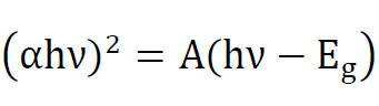
where α is the absorption coefficient, hν is the photon energy, and A is a constant [39]. The absorption coefficient was calculated using the Eq. 2:
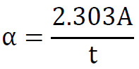
where A is the absorbance and t is the film thickness [40]. The photon energy was calculated using Eq. 3:
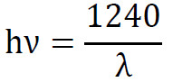
Plotting (𝛼ℎ𝜈)2 versus photon energy ℎ𝜈 and extending the linear part of the curve to intersect the energy axis yielded the optical band gap. The third concentration of Ag doping in ZnO/Ag in this investigation was 9.0g/L, and the corresponding film thickness for this concentration was determined to be roughly 8.94 nm, which was utilized to compute the absorption coefficient [41]. Only this thickness value was chosen, to do with the sample having the highest post-filtration concentration (9.0g/L), for which we constructed their tauc plot, then determined their optical band gap. The Tauc plot of (αhν)2 versus hν is shown in Fig. 6.
The Tauc plot shows a linear region, which indicates a direct band gap transition in ZnO: Ag thin films. The estimated band gap value is about 3.33 eV, and this result is consistent with previously reported values for doped ZnO thin films, which usually fall within the range of 3.2–3.5 eV [42].
Gas Sensing System Description
The detection performance of the sensors fabricated at different temperatures was investigated toward NO₂ gas (150 ppm) within an operating temperature range between (RT -100 -200°C). The heater also allowed for electrical and thermocouple connections to the sensor inside a sealed test chamber. The chamber was evacuated down to 10^-1 bar using a rotary pump. A temperature controller was responsible for regulating the desired temperature, while flow meters and needle valves were used to adjust the carrier air and test gas flow rates. The chamber was then filled with a known concentration of the target gas, and the resistance change of the sensor was measured. After a measurement, the test gas valve was closed and left to recover or return to baseline resistance in dry air. Sensor response was calculated from Eq. 4.
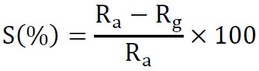
where Ra and Rg are the sensor resistances in dry air and target gas, respectively [43].
Dynamic Resistance–Time Behavior
Figs. 7 a–c presents the dynamic resistance–time curves of Pure ZnO and ZnO + Ag sensors toward 150 ppm NO₂ gas at different operating temperatures (RT, 100 °C, and 200 °C). At room temperature (RT), both samples exhibit a noticeable change in resistance upon exposure to NO₂ gas. The dynamic resistance–time curves recorded at room temperature, 100°C, and 200°C demonstrate the significant influence of operating temperature on the sensing performance of pure and doped ZnO sensors toward 150 ppm NO₂ gas. At room temperature, the resistance increases upon exposure to NO₂ due to its electron-withdrawing nature, where NO₂ molecules extract electrons from the conduction band of n-type ZnO, resulting in the expansion of the depletion layer and a corresponding increase in resistance. This sensing mechanism and the role of surface charge modulation in ZnO-based gas sensors have been widely reported in recent studies [44,45]. When the gas is removed, and the sensor is exposed to clean air, the resistance gradually returns toward its baseline value, reflecting the typical response–recovery behavior governed by adsorption–desorption kinetics. At 100°C, the response–recovery cycles become sharper and faster compared to room temperature, with steeper slopes and shorter time intervals between consecutive peaks. This behavior indicates enhanced adsorption–desorption kinetics and accelerated surface reaction rates at elevated temperature, as discussed in recent reviews on ZnO-based gas sensors [45]. At 200°C, the highest resistance modulation is observed, particularly for the doped samples. The enhanced response amplitude suggests improved catalytic activity and more efficient charge transfer processes at higher temperatures. Recent investigations confirm that doping and heterojunction engineering significantly enhance NO₂ sensing performance by improving surface reactivity and electron transport properties. Overall, the doped ZnO sensor exhibits larger resistance variation compared to pure ZnO at all operating temperatures, confirming that dopant incorporation enhances gas adsorption and sensing efficiency [44,46]. Moreover, the time interval between two consecutive peaks represents the complete sensing cycle (response and recovery times), which decreases progressively with increasing temperature due to improved adsorption–desorption kinetics [45]. At 100 °C, the response–recovery cycles become sharper and faster, indicating improved adsorption–desorption kinetics for both samples.
Gas Sensitivity
Fig. 8 shows the sensitivity values of Pure ZnO and ZnO + Ag sensors toward 150 ppm NO₂ gas at different operating temperatures (25 °C, 100 °C, and 200) Fig. 8 illustrates the variation in sensitivity values of pure ZnO and doped ZnO sensors toward 150 ppm NO₂ gas at different operating temperatures (25°C, 100°C, and 200°C). It is observed that the sensitivity of pure ZnO gradually increases with increasing temperature, indicating that elevated temperature enhances surface reaction kinetics and improves adsorption–desorption processes, as reported in recent studies on ZnO thin films and nanostructures [47,48]. In contrast, the doped ZnO sensor exhibits a significant enhancement in sensitivity at moderate temperature, followed by a slight decrease at 200°C. This improvement can be attributed to the catalytic effect of dopants, which increases the number of active adsorption sites and facilitates charge transfer between NO₂ molecules and the sensing surface [47,49]. The slight reduction in sensitivity at higher temperatures may result from accelerated desorption of gas molecules, which reduces the effective interaction time between NO₂ and the sensor surface [48]. Overall, the results confirm that structural modification or doping of ZnO significantly enhances NO₂ sensing performance compared to pure ZnO. Furthermore, operating temperature plays a crucial role in determining the sensor response and recovery efficiency, consistent with recent reports on ZnO-based NO₂ gas sensors [47,49].
Response and Recovery Time
The response time (t₉₀) is defined as the time required for the sensor to reach 90% of the total resistance change upon exposure to 150 ppm NO₂ gas. The recovery time is defined as the time required for the sensor to return to 90% of its initial resistance value after removal of the target gas. Fig. 9 shows that the (ZnO+Ag) sensor exhibits a shorter response time compared to pure ZnO, particularly at 100°C, indicating enhanced surface reaction kinetics after Ag incorporation. The decoration of ZnO with Ag nanoparticles increases the number of active adsorption sites and promotes catalytic activation of NO₂ molecules, leading to faster charge transfer and improved dynamic sensing performance [50]. From a mechanistic perspective, the improvement is attributed to the formation of a Schottky junction at the Ag/ZnO interface due to the work function difference between metallic Ag and n-type ZnO. This metal–semiconductor junction enhances electron trapping and strengthens depletion layer modulation during NO₂ adsorption, resulting in faster resistance variation and improved response–recovery characteristics [51]. Overall, Ag decoration significantly enhances the dynamic sensing behavior compared to pure ZnO.
Table 2 clearly shows that the sensing behavior of both samples is strongly dependent on temperature. For pure ZnO, the sensitivity is linearly increased with increasing temperature, achieving a peak value of 51.71% at 200 °C with significant reduction of response time from 19.08 s at RT to as low as 9.9 s at 200 °C indicating that both surface reaction kinetics are considerably improved with the presence of elevated temperatures. In contrast to this, ZnO + Ag sample shows maximum sensitivity at 100 °C (51.78%) with the decrease in sensitivity at 200 °C (43.1%). The sensitivity of pure ZnO starts to be higher than that of the Ag-modified sample at 200 °C, which suggests that high temperature may induce too much desorption of NO₂ molecules from the surface modified by Ag and a fewer number of the active adsorbed species that participated in charge transfer. Despite the fact that the response time of ZnO + Ag at elevated temperatures was longer than that of pure ZnO, their recovery times stayed more constant (relative to the former) as observed in the figure which suggests different surface reaction dynamics following identical metal incorporation. Thus, the optimal operating temperature for Ag modification changes to 100 °C, while pure ZnO shows superior gas-sensing at high temperatures.
CONCLUSION
Herein, we have synthesized and characterized nano-crystalline ZnO and Ag-doped ZnO films by the spin coating method for NO₂ gas sensing application. It was evident from the results that both thermal annealing and Ag doping are significant in improving structural, optical, and sensing properties of ZnO-based thin films. SEM analysis of the samples showed that annealing reduced agglomeration and increased grain uniformity with each particle. Ag incorporation was found to increase surface area further, along with a connection between particles. Annealing also suppresses the structural defects and enhances the transmittance, suggesting that it improves crystallinity and film quality, as shown by both optical measurements. The sensing results demonstrated that Ag doping greatly improved the gas sensing performance of ZnO. Compared with pristine sensors, the doped sensor possessed a superior sensitivity, rapid response–recovery pattern as well as outstanding moderate operating temperature (particularly at 100 °C) performance, which was due to the catalytic activity of Ag nanoparticles, growth of adsorption sites and advancement charge transfer transport sectors. In summary, the process of fabricating ZnO via spin coating combined with thermal annealing and Ag doping represents a powerful approach to advance the performance of NO₂ gas sensors for improved air quality monitoring. This study substantiates the potential of Ag–ZnO thin films for practical application in environmental monitoring and smart sensing applications.
CONFLICT OF INTEREST
The authors declare that there is no conflict of interests regarding the publication of this manuscript.
